1. Basic Computer Organization¶ Open the notebook in Colab
(C) Copyright Notice: This chapter is part of the book available athttps://pp4e-book.github.io/and copying, distributing, modifying it requires explicit permission from the authors. See the book page for details:https://pp4e-book.github.io/
In this chapter, we will provide an overview of the internals of a modern computer. To do so, we will first describe a general architecture on which modern computers are based. Then, we will study the main components and the principles that allow such machines to function as general purpose “calculators”.
1.1. The von Neumann Architecture
1.1.1. John von Neumann
From: Oxford Reference “Hungarian-born US mathematician, creator of the theory of games and pioneer in the development of the modern computer. Born in Budapest, the son of a wealthy banker, von Neumann was educated at the universities of Berlin, Zürich, and Budapest, where he obtained his PhD in 1926. After teaching briefly at the universities of Berlin and Hamburg, von Neumann moved to the USA in 1930 to a chair in mathematical physics at Princeton. In 1933, he joined the newly formed Institute of Advanced Studies at Princeton as one of its youngest professors. By this time he had already established a formidable reputation as one of the most powerful and creative mathematicians of his day. In 1925 he had offered alternative foundations for set theory, while in his Mathematischen Grundlagen der Quantenmechanik (1931) he removed many of the basic doubts that had been raised against the coherence and consistency of quantum theory. In 1944, in collaboration with Oskar Morgenstern (1902–77), von Neumann published The Theory of Games and Economic Behaviour. A work of great originality, it is reputed to have had its origins at the poker tables of Princeton and Harvard. The basic problem was to show whether it was possible to speak of rational behaviour in situations of conflict and uncertainty as in, for example, a game of poker or wage negotiations. In 1927 von Neumann proved the important theorem that even in games that are not fully determined, safe and rational strategies exist. With entry of the USA into World War II in 1941 von Neumann, who had become an American citizen in 1937, joined the Manhattan project (for the manufacture of the atom bomb) as a consultant. In 1943 he became involved at Los Alamos on the crucial problem of how to detonate an atom bomb. Because of the enormous quantity of computations involved, von Neumann was forced to seek mechanical aid. Although the computers he had in mind could not be made in 1945, von Neumann and his colleagues began to design Maniac I (Mathematical analyser, numerical integrator, and computer). Von Neumann was one of the first to see the value of a flexible stored program: a program that could be changed quite easily without altering the computer’s basic circuits. He went on to consider deeper problems in the theory of logical automata and finally managed to show that self-reproducing machines were theoretically possible. Such a machine would need 200 000 cells and 29 distinct states. Having once been caught up in affairs of state von Neumann found it difficult to return to a purely academic life. Thereafter much of his time was therefore spent, to the regret of his colleagues, advising a large number of governmental and private institutions. In 1954 he was appointed to the Atomic Energy Commission. Shortly after this, cancer was diagnosed and he was forced to struggle to complete his last work, the posthumously published The Computer and the Brain (1958).” | 
Fig. 1.1.1 John von Neumann (1903 – 1957)¶ |
1.1.2. Components of the von Neumann Architecture
The von Neumann architecture (Fig. 1.1.2) defines the basic structure, or outline, used in most computers today. Proposed in 1945 by von Neumann, it consists of two distinct units: An addressable memory and a Central Processing Unit (CPU). All the encoded actions and data are stored together in the memory unit. The CPU, querying these actions, the so-called instructions, executes them one by one, sequentially (though, certain instructions may alter the course of execution order).
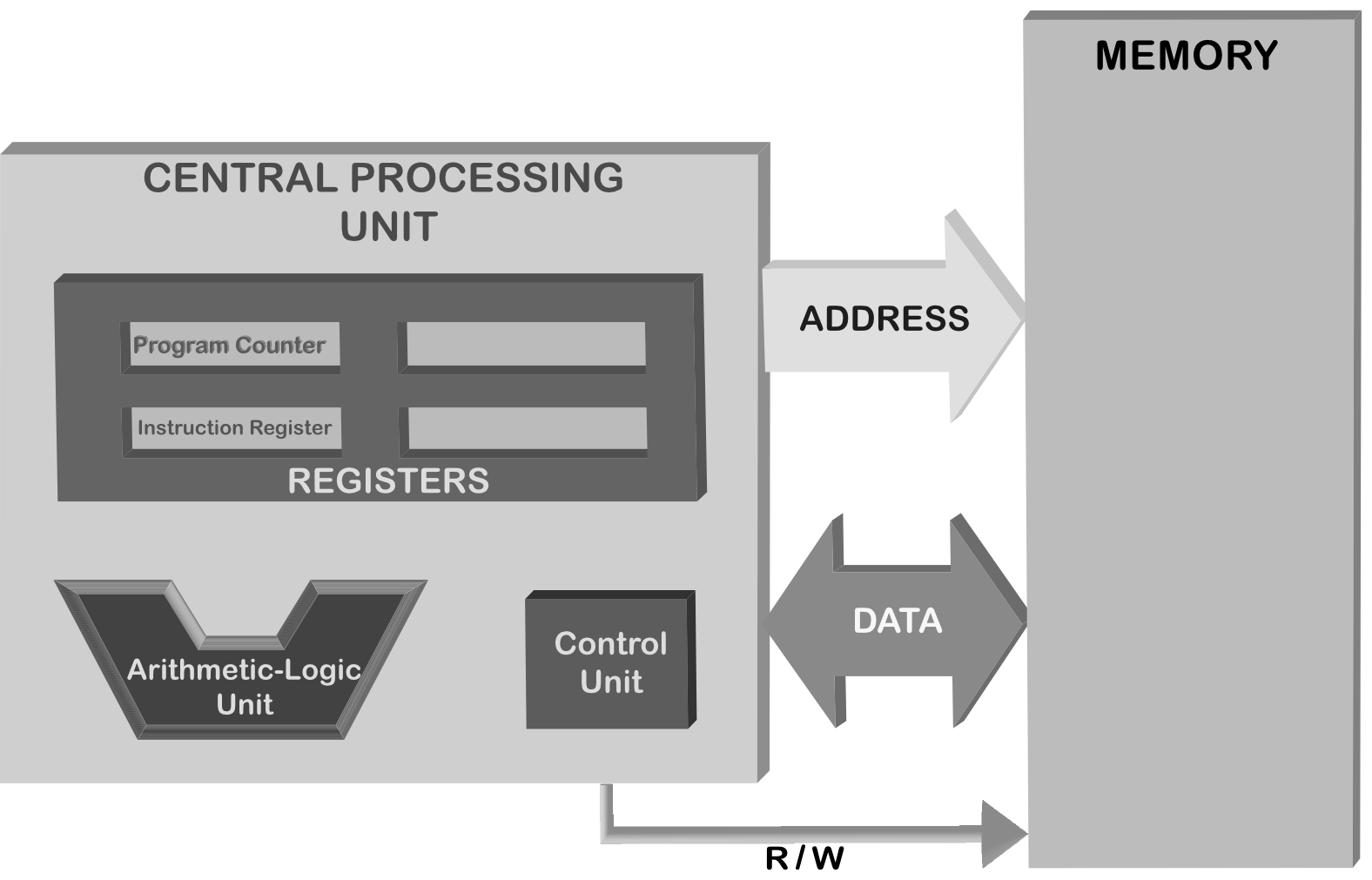
Fig. 1.1.2 A block structure view of the von Neumann Architecture.
The CPU communicates with the memory via two sets of wires, namely the
address bus and the data bus, plus a single R/W wire
(Fig. 1.1.2). These busses consist of several wires and
carry binary information to/from the memory. Each wire in a bus carries
one bit of the information (either a zero (0) or a one (1)).
Today’s von Neumann architectures are working on electricity, and
therefore, these zeros and ones correspond to voltages. A one indicates
usually the presence of a 5V and a zero denotes the absence of it.
1.2. The Memory
The memory can be imagined as pigeon holes organized as rows
(Fig. 1.2.1). Each row has eight pigeon holes, each
being able to hold a zero (0) or one (1) – in electronic terms,
each pigeon hole is capable of storing a voltage (can you guess what
type of an electronical component a pigeon hole is?). Each such row is
named to be of the size byte; i.e., a byte means 8 bits.
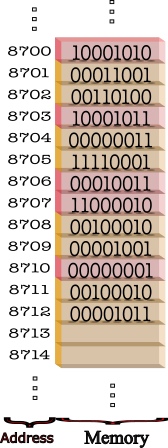
Fig. 1.2.1 The memory is organized as a stack of rows such that each row has an associated address.
Each byte of the memory has a unique address. When the address input
(also called address bus – Fig. 1.1.2) of the memory is
provided a binary number, the memory byte that has this number as the
address becomes accessible through the data output (also called output
data bus). Based on W/R wire being set to Write (1) or Read (0),
the action that is carried out on the memory byte differs:
- W/R wire is set to WRITE (1) :The binary content on the input data bus is copied into the 8-bit location whose address is provided on the address bus, the former content is overwritten.
- W/R wire is set to READ (0) :The data bus is set to a copy of the content of 8-bit location whose address is provided on the address bus. The content of the accessed byte is left intact.
The information stored in this way at several addresses live in the memory happily, until the power is turned off.
The memory is also referred as Random Access Memory (RAM). Some important aspects of this type of memory have to be noted:
Accessing any content in RAM, whether for reading or writing purposes, is only possible when the content’s address is provided to the RAM through the address bus.
Accessing any content takes exactly the same amount of time, irrespective of the address of the content. In todays RAMs, this access time is around 50 nanoseconds.
When a content is overwritten, it is gone forever and it is not possible to undo this action.
An important question is who sets the address bus and communicates through the data bus (sends and receives bytes of data). As depicted in Fig. 1.1.2, the CPU does. How this is done on the CPU side will become clear in the next section.
1.3. The CPU
The Central Processing Unit, which can be considered as the ‘brain’ of a computer, consists of the following units:
Control Unit (CU), which is responsible for fetching instructions from the memory, interpreting (‘decoding’) them and executing them. After executing an instruction finishes, the control unit continues with the next instruction in the memory. This “fetch-decode-execute” cycle is constantly executed by the control unit.
Arithmetic Logic Unit (ALU), which is responsible for performing arithmetic (addition, subtraction, multiplication, division) and logic (less-than, greater-than, equal-to etc.) operations. CU provides the necessary data to ALU and the type of operation that needs to be performed, and ALU executes the operation.
Registers, which are mainly storage units on the CPU for storing the instruction being executed, the affected data, the outputs and temporary values.
The size and the quantity of the registers differ from CPU model to model. They generally have size in the range of [2-64] bytes and most registers on today’s most popular CPUs have size 64 bits (i.e. 8 bytes). Their quantity is not high and in the range of [10-20]. The registers can be broadly categorized into two: Special Purpose Registers and General Purpose Registers.
Two special purpose registers are worth mentioning to understand how a CPU’s Fetch-Decode-Execute cycle runs. The first is the so-called Program Counter (PC) and the second is the Instruction Register (IR).
Input/Output connections, which connect the CPU to the other components in the computer.
1.4. The Fetch-Decode-Execute Cycle
The CPU is in fact a state machine, a machine that has a representation of its current state. The machine, being in a state, reads the next instruction and executes the instruction according to its current state. The state consists of what is stored in the registers. Until it is powered off, the CPU follows the Fetch-Decode-Execute cycle (Fig. 1.4.1) where each step of the cycle is based on its state. The control unit is responsible for the functioning of the cycle.

Fig. 1.4.1 The CPU constantly follows the fetch-decode-execute cycle while the computer is running a program.
1- The Fetch Phase
The cycle starts with the Fetch Phase. At the beginning of this phase, the CPU has the address (the position in the memory) of the next instruction in the PC (Program Counter) Register. During this phase, the address bus is set to this address in the PC register and the R/W wire is set to Read (0). The memory responds to this by providing the memory content at the given address on the data bus.
How many bytes are sent through the data bus is architecture dependent. Usually it is 4-8 bytes. These bytes are received into the IR (Instruction Register).
2- The Decode Phase
At the beginning of this phase, the IR is assumed to be holding the current instruction. The content of the first part of the IR electronically triggers some action. Every CPU has an electronically built-in hard-wired instruction table in which every possible atomic operation that the CPU can carry out has an associated binary code, called operation code (opcode in short). This table differs from CPU brand to brand.
There are three types of instructions:
Data manipulation: Arithmetic/Logic operations on/among registers,
Data transfer: Memory-to-Register, Register-to-Memory, Register-to-Register transfers,
Control flow of execution: Instructions that stop execution, jump to a different part of the memory for next instruction, instead of the next one in the memory.
Let us assume that our instruction looks like this:
Opcode |
Effected data or address |
|---|---|
0001 |
0110 |
This is an 8-byte instruction that has the first 4 bits as representing
the opcode. The designer could have designed the CPU such that the
opcode 0001 denotes an instruction for reading data from the memory,
writing data to the memory or adding the contents of the two registers
etc. The remaining four bits then contain the parameters of the
instruction, which are the data to be operated on, the address in the
memory or the codes of the registers etc.
Let us assume that this 8-bit example instruction (i.e. the opcode
0001) denotes an addition on two registers and that the remaining 4
bits encode the registers in question, with 01 denoting one register
and 10 the other register. Prior to the instruction, we can assume
the two registers to contain integers, and after the instruction is
executed, one of the registers will be incremented by the amount of the
other (by means of integer addition).
Although this was a simple and hypothetical example, it illustrates how modern CPUs can decode an instruction and decipher its elements. Though, the length of an instruction and the variety of instructions are clearly different.
3- The Execute Phase
As the name implies, the electronically activated and initialized circuitry carries out the instruction in this phase. Depending on the instruction, the registers, the memory or other components are effected. When the instruction completes, the PC is updated by one unless it was a control flow changing instruction in which case the PC is updated to the to-be-jumped address in the memory (in some designs, the PC can be updated in the fetch phase, after fetching the instruction). Not all instructions take the same amount of time to be carried out. Floating point division, for example, takes much more time compared to others.
A CPU goes through the Fetch-Decode-Execute cycle until it is powered off. What happens at the very beginning? The electronics of the CPU is manufactured such that, when powered up, the PC register has a very fixed content. Therefore, the first instruction is always fetched from a certain position.
An intelligent question would be “when does the CPU jump from one state to another?”. One possible answer is: whenever the previous state is completed electronically, a transition to the next state is performed. Interestingly, this is not true. The reality is that there is an external input to the CPU from which electronic pulses are fed. This input is called the system clock and each period of it is named as a clock cycle. The best performance would be that each phase of the fetch-decode-execute cycle is completed in one-and-only-one clock cycle. On modern CPUs, this is true for addition instruction, for example. But there are instructions (like floating point division) which take about 40 clock cycles.
What is length of a clock cycle? CPUs are marked with their clock frequency. For example, Intel’s latest processor, i9, has a maximal clock frequency of 5GHz (that is \(5\times 10^9\) pulses per second). So, since \(\mbox{(period)} = 1/\mbox{(frequency)}\), for this processor a clock cycle is 200 pico seconds. This is such a short time that light would travel only 6 cm.
A modern CPU has many more features and functional components: interrupts, ports, various levels of caches are a few of them. To cover them is certainly out of the scope of this course material.
1.5. The Stored Program Concept
In order for the CPU to compute something, the corresponding instructions to do the computation have to be placed into the memory (how this is achieved will become clear in the next chapter). These instructions and data that perform a certain task are called a Computer Program. The idea of storing a computer program into the memory to be executed is coined as the Stored Program Concept.
What does a stored program look like? Below you see a real extract from the memory, a program that multiplies two integer numbers sitting in two different locations in the memory and stores the result in another memory location (to save space consecutive 8 bytes in the memory are displayed in a row, the next row displays the next 8 bytes):
01010101 01001000 10001001 11100101 10001011 00010101 10110010 00000011
00100000 00000000 10001011 00000101 10110000 00000011 00100000 00000000
00001111 10101111 11000010 10001001 00000101 10111011 00000011 00100000
00000000 10111000 00000000 00000000 00000000 00000000 11001001 11000011
...
11001000 00000001 00000000 00000000  00000000 00000000
Unless you have a magical talent, this should not be understandable to you. It is difficult because it is just a sequence of bytes. Yes, the first byte is presumably an instruction, but what is it? Furthermore, since we do not know what it is, we do not know whether it is followed by some data or not, so we cannot say where the second instruction starts. However, the CPU for which these instructions were written for would know this, hard-wired in its electronics.
When a programmer wants to write a program at this level, i.e. in terms of binary CPU instructions and binary data, s/he has to understand and know each instruction the CPU can perform, should be able to convert data to some internal format, to make a detailed memory layout on paper and then to start writing down each bit of the memory. This way of programming is an extremely painful job; though it is possible, it is impractical.
Alternatively, consider the text below:
main:
       pushq   %rbp
       movq    %rsp, %rbp
       movl    alice(%rip), %edx
       movl    bob(%rip), %eax
       imull   %edx, %eax
       movl    %eax, carol(%rip)
       movl    $0, %eax
       leave
       ret
alice:
       .long   123
bob:
       .long   456
Though pushq and moveq are not immediately understandable, the
rest of the text provides some hints. alice and bob must be some
programmer’s name invention, e.g. denoting variables with values 123
and 456 respectively; imull must have something to do with
‘multiplication’, since only registers can be subject to arithmetic
operations; %edx and %eax must be some denotation used for
registers; having uncovered this, movls start to make some sense:
they are some commands to move around data… and so on. Even without
knowing the instruction set, with a small brainstorming we can uncover
the action sequence.
This text is an example assembly program. A human invented denotation for instructions and data. An important piece of knowledge is that each line of the assembler text corresponds to a single instruction. This assembly text is so clear that even manual conversion to the cryptic binary code above is feasible. Form now on, we will call the binary code program as a Machine Code Program (or simply the machine code).
How do we automatically obtain machine codes from assembly text? We have machine code programs that convert the assembly text into machine code. They are called Assemblers.
Despite making programming easier for programmers, compared to machine codes, even assemblers are insufficient for efficient and fast programming. They lack some high-level constructs and tools that are necessary for solving problems easier and more practical. Therefore higher level languages that are much easier to read and write compared to assembly are invented.
We will cover the spectrum of programming languages in more detail in the next chapter.
1.6. Pros and Cons of the von Neuman Architecture
The von Neumann architecture has certain advantages and disadvantages:
Advantages
CPU retrieves data and instruction in the same manner from a single memory device. This simplifies the design of the CPU.
Data from input/output (I/O) devices and from memory are retrieved in the same manner. This is achieved by mapping the device communication electronically to some address in the memory.
The programmer has a considerable control of the memory organization. So, s/he can optimize the memory usage to its full extent.
Disadvantages
Sequential instruction processing nature makes parallel implementations difficult. Any parallelization is actually a quick sequential change in tasks.
The famous “Von Neumann bottleneck” : Instructions can only be carried out one at a time and sequentially.
Risk of an instruction being unintentionally overwritten due to an error in the program.
An alternative to the von Neumann Architecture is the Harvard Architecture which could not resist the test of time due to crucial disadvantages compared to the von Neumann architecture.
1.7. Peripherals of a computer
Though it is somewhat contrary to your expectation, any device outside of the von Neumann structure, namely the CPU and the Memory, is a peripheral. In this aspect, even the keyboard, the mouse and the display are peripherals. So are the USB and ethernet connections and the internal hard disk. Explaining the technical details of how those devices are connected to the von Neumann architecture is out of the scope of this book. Though, we can summarize it in a few words.
All devices are electronically listening to the busses (the address and data bus) and to a wire running out of the CPU (which is not pictured above) which is 1 or 0. This wire is called the port_io line and tells the memory devices as well as to any other device that listens to the busses whether the CPU is talking to the (real) memory or not. If it is talking to the memory all the other listeners keep quiet. But if the port_io line is 1, meaning the CPU doesn’t talk to the memory but to the device which is electronically sensitive to that specific address that was put on the address bus (by the CPU), then that device jumps up and responds (through the data bus). The CPU can send as well as receive data from that particular device. A computer has some precautions to prevent address clashes, i.e. two devices responding to the same address information in port_io.
Another mechanism aids communication requests initiated from the peripherals. Of course it would be possible for the CPU from time to time stop and do a port_io on all possible devices, asking them for any data they want to send in. This technique is called polling and is extremely inefficient for devices that send asynchronous data (data that is send in irregular intervals): You cannot know when there will be a keyboard entry so, in polling, you have to ask very frequently the keyboard device for the existence of any data. Instead of dealing with the inefficiency of polling, another mechanism is built into the CPU. The interrupt mechanism is an electronic circuitry of the CPU which has inlets (wires) connected to the peripheral devices. When a device wants to communicate with (send or receive some data to/from) the CPU they send a signal (1) from that specific wire. This gets the attention of the CPU, the CPU stops what it is doing at a convenient point in time, and asks the device for a port_io. So the device gets a chance to send/receive data to/from the CPU.
1.8. The running of a computer
When you power on a computer, it first goes through a start-up process (also called booting), which, after performing some routine checks, loads a program from your disk called Operating System.
1.8.1. Start up Process
At the core of a computer is the von Neumann architecture. But how a machine code finds its way into the memory, gets settled there, so that the CPU starts executing it, is still unclear.
When you buy a brand new computer and turn it on for the first time, it does some actions which are traceable on its display. Therefore, there must be a machine code in a memory which, even when the power is off, does not lose its content, very much like a flash drive. It is electronically located exactly at the address where the CPU looks for its first instruction. This memory, with its content, is called Basic Input Output System, or in short BIOS. In the former days, the BIOS was manufactured as write-only-once. To change the program, a chip had to be replaced with a new one. The size of the BIOS of the first PCs was 16KB, nowadays it is about 1000 times larger, 16MB.
When you power up a PC the BIOS program will do the following in sequence:
Power-On Self Test, abbreviated as POST, which determines whether the CPU and the memory are intact, identifies and if necessary, initializes devices like the video display card, keyboard, hard disk drive, optical disc drive and other basic hardware.
Looking for an operating system (OS): The BIOS program goes through storage devices (e.g. hard disk, floppy disk, USB disk, CD-DVD drive, etc.) connected to the computer in a predefined order (this order is generally changeable by the user) and looks for and settles for the first operating system that it can find. Each storage device has a small table at the beginning part of the device, called the Master Boot Record (MBR), which contains a short machine code program to load the operating system if there is one.
When BIOS finds such a storage device with an operating system, it loads the content of the MBR into the memory and starts executing it. This program loads the actual operating system and then runs it.
BIOS is nowadays replaced by Unified Extensible Firmware Interface (UEFI) which introduces more capabilities such as faster hardware check, better user interface and more security. With UEFI, MBR is replaced by GPT (Globally-unique-identifier Partition Table) to allow larger disks, larger partitions (drives) and better recovery options.
1.8.2. The Operating System
The operating system is a program that, after being loaded into the memory, manages resources and services like the use of memory, the CPU and the devices. It essentially hides the internal details of the hardware and makes the ugly binary machine understandable and manageable to us.
An OS has the following responsibilities:
Memory Management: Refers to the management of the memory connected to the CPU. In modern computers, there is more than one machine code program loaded into the memory. Some programs are initiated by the user (like a browser, document editor, Word, music player, etc.) and some are initiated by the operating system. The CPU switches very fast from one program (this is called a process) in the memory to another. The user (usually) does not feel the switching. The memory manager keeps track of the space allocated by processes in the memory. When a new program (process) is being started, it has to be placed into the memory. The memory manager decides where it is going to be placed. Of course, when a process ends, the place in the memory occupied by the process has to be reclaimed; that is the memory manager’s job. It is also possible that, while running, a process demands additional space in the memory (e.g. a photoshop-like program needs more space for a newly opened JPG image file) then the process makes this demand to the memory manager, which grants it or denies it.
Process (Time) Management: As said above, a modern memory generally contains more than one machine code program. An electronic mechanism forces the CPU to switch to the Time Manager component of the OS. At least 20 times a second, the time manager is invoked to make a decision on behalf of the CPU: Which of the processes that sit in the memory will be run during the next period? When a process gets the turn, the current state of the CPU (the contents of all registers) is saved to some secure position in the memory, in association to the last executing process. From that secure position, the last saved state information which going to take the turn is found and the CPU is set to that state. Then the CPU, for a period of time executes that process. At the end of that period, the CPU switches over to the time manager and the time manager makes a decision for the next period. Which process will get the turn? And so on. This decision making is a complex task. Still there are Ph.D. level research going on on this subject. The time manager collects some statistics about each individual process and its system resource utilization. Also there is the possibility that a process has a high priority associated due to several reasons. The time manager has to solve a kind of optimization problem under some constraints. As mentioned, this is a complex task and a hidden quality factor of an OS.
Device Management: All external devices of a computer have a software plug-in to the operating system. An operating system has some standardized demands from devices and these software plug-ins implement these standardized functionality. This software is usually provided by the device manufacturer and is loaded into the operating system as a part of the device installing process. These plug-ins are named as device drivers.
An Operating System performs device communication by means of these drivers. It does the following activities for device management:
Keeps tracks of all devices’ status.
Decides which process gets access to the device when and for how long.
Implements some intelligent caching, if possible, for the data communication with the device.
De-allocates devices.
File Management: A computer is basically a data processing machine. Various data are produced or used for very diverse purposes. Textual, numerical, audio-visual data are handled. Handling data also includes storing and retrieving it on some external recording device. Examples for such recording devices are hard disks, flash drives, CDs and DVDs. Data is stored on these devices as files. A file is a persistent piece of information that has a name, some meta data (e.g. information about the owner, the creation time, size, content type, etc.) and the data.
The organizational mechanism for how files are stored on devices is called the file system. There are various alternatives to do this. FAT16, FAT32, NTFS, EXT2, EXT3, ExFAT, HFS+ are a few of about a hundred (actually the most common ones). Each has its own pros and cons as far as max allowed file size, security, robustness (repairability), extensibility, metadata, lay out policies and some other aspects are concerned. Files are most often managed in a hierarchy. This is achieved by a concept of directories or folders. On the surface (as far as the user sees them), a file system usually consist of files separated into directories where directories can contain files or other directories.
The file manager is responsible for creation & initialization of a file system, inclusion and removal of devices from this system and management of all sorts of changes in the file system: Creation, removal, copying of files and directories, dynamically assigning access rights for files and directories to processes etc.
Security: This is basically for the maintenance of the computer’s integrity, availability, and confidentiality. The security of a computer exists at various layers such as:
maintaining the physical security of the computer system,
the security of the information the system is in hold of, and
the security of the network to which the computer is connected.
In all of these, the operating system plays a vital role in keeping the security. Especially the second item is where the operating system is involved at most. Information, as you know by now, is placed in the computer in two locations. The internal memory and the external storage devices. The internal memory is in hold of the processes and the processes should not interfere with each other (unless specifically intended). Actually in a modern day computer, there can be more than one user working at the same time on the computer. Their processes running in the memory as well as their files being on the file system must remain extremely private and separate. Even their existence has to be hidden from every other user.
Computers are connected and more and more integrated in a global network. This integration is done on a spectrum of interactions. In the extreme case, a computer can be solely controlled over the network. Of course this is done by supplying some credentials but, as you would guess, such a system is prone to malicious attacks. An operating system has to take measures to protect the computer system from such harms. Sometimes it is the case that bugs of the OS are discovered and exploited in order to breach security.
User Interface: As the computer’s user, when you want to do anything you do this by ordering the operating system to do it. Starting/terminating a program, exploring or modifying the file system, installing/uninstalling a new device are all done by “talking” to the operating system. For this purpose, an OS provides an interface, coined as the user interface. In the older days, this was done by typing some cryptic commands into a typewriter at a console device. Over the years, the first computer with a Graphical User Interface (GUI) emerged. A GUI is a visual interface to the user where the screen can host several windows each dedicated to a different task. Elements of the operating system (processes, files, directories, devices, network communications) and their status are symbolized by icons and the interactions are mostly via moving and clicking a pointing device which is another icon (usually a movable arrow) on the screen. The Xerox Alto introduced on March 1973 was the first computer that had a GUI. The first personal computer with a GUI was Apple Lisa, introduced in 1983 with a price of $10,000. Almost three years later, by the end of 1985, Microsoft released its first OS with a GUI: Windows 1.0. The archaic console typing still exists, in the form a type-able window, called terminal, which is still very much favoured among programming professionals because it provides more control for the OS.
1.9. Important Concepts
We would like our readers to have grasped the following crucial concepts and keywords from this chapter:
The von Neumann Architecture.
The interaction between the CPU and the memory via address, R/W and data bus lines.
The crucial components on the CPU: The control unit, the arithmetic logic unit and the registers.
The fetch-decode-execute cycle.
The stored program concept.
Operating system and its responsibilities.
1.10. Further Reading
Computer Architectures:
Von Neumann Architecture: http://en.wikipedia.org/wiki/Von_Neumann_architecture
Harvard Architecture: http://en.wikipedia.org/wiki/Harvard_architecture
Harvard vs. Von Neumann Architecture: http://www.pic24micro.com/harvard_vs_von_neumann.html
Quantum Computer: http://en.wikipedia.org/wiki/Quantum_computer
Chemical Computer: http://en.wikipedia.org/wiki/Chemical_computer
Non-Uniform Memory Access Computer: http://en.wikipedia.org/wiki/Non-Uniform_Memory_Access
Running a computer:
Booting a computer: https://en.wikipedia.org/wiki/Booting
History of operating systems: https://en.wikipedia.org/wiki/History_of_operating_systems
Operating systems: https://en.wikipedia.org/wiki/Operating_system
1.11. Exercises
To gain more insight, play around with the von Neumann machine simulator at http://vnsimulator.altervista.org
Using Google and the manufacturer’s web site, find the following information for your desktop/laptop:
Memory (RAM) size
CPU type and Clock frequency
Data bus size
Address bus size
Size of the general purpose registers of the CPU
Harddisk or SSD size and random access time
Opcode |
Affected address |
|---|---|
0001 |
0100 |
Assume that we have a CPU that can execute instructions with the format and size given above.
What is the number of different instructions that this CPU can decode?
What is the maximum number of rows in the memory that can be addressed by this CPU?